
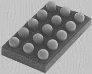
Wafer Level CSP
Overview
Due to the market trend of semiconductor package miniaturization, WLCSP is the solution, which provides low cost, smaller scale, stable transmission and better heat dissipation benefits. GTK provides a full turnkey solution of WLCSP, including bumping, wafer probe, and DPS
| Type | Die Size (mm) | Die Thickness (mm) | Bump Size (mm) | Bump Diameter (mm) |
| WLCSP | 0.61 〜5.975 | 0.150 〜0.425 | 0.150-0.300 | Max. 0.315 |
Feature
- 8 inch & 12 inch.
- Thinning, backside lamination, laser marking, (laser) sawing,and tape-and-reel.
- Application: communication, PMIC, Controller, handset audio.
Packing method
Tape & Reel/ Waffle pack