
Flip Chip CSP
Overview
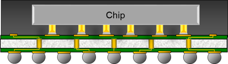
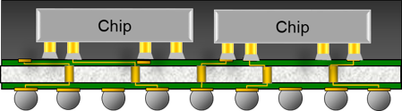
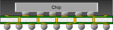
“FCCSP packages form a subgroup of the Flip Chip package family of the form factor known as Chip Scale Packages (CSP). This package construction partners with all of our available bumping options (Copper Pillar, Pb-free solder), while enabling flip chip interconnect technology in area array and, when replacing standard wirebond interconnect, in a peripheral bump layout. The advantages of flip chip interconnect are multiple: it provides enhanced electrical performance over standard wirebond technology.
Greatek offers a complete line of FCCSP products, with package sizes from 3×3 to 10X10mm, developed to fulfill customers’ requests”
Feature
- Body sizes 3 x 3mm through 10 x10mm.
- Electroplated Pb-free or Cu pillar bumps.
- Bumping capability down to 160µm pitch with lead-free solder and pitch down to 120µm with Cu pillar.
- Full service wafer bumping PI dielectric options for wafer repassivation and redistribution layer (RDL).
- Molded underfill (MUF) available.
- MUF with solder bump and Cu pillar bump qualified and in production.
- BGA/LGA ball pitch 0.40mm qualified and in production.
- Maximum overall height of 1.00mm (FCCSP) ; 0.90mm (FCCSP) ; 0.68mm (FCLGA).
- Conventional 2 to 4layer through-hole or PPG build-up laminate substrates available.
- Molded Interconnect Substrate (MIS) in HVM, No-Clean Flux qualified and HVM.
Package Configurations
| Body Sizes(mm) | 3×3 to 10×10 with square or rectangular body size options; |
| Ball Count | 200 to 500 |
| Ball Pitch (mm) | 0.4 to 0.65 |
| Typ. Pkg. Thickness | FCCSP: 1.00mm max FCCSP : 0.90mm max. FCLGA : 0.68mm max. |
Packing method
JEDEC Tray / Tape & Reel available.
Reliability Qualification
| Moisture Sensitivity Level | JEDEC MSL3 (30°C / 60% RH / 192hrs) |
| Temp. Cycle Test | -65/+150°C, 500 cycles |
| Pressure Cooker Test | 121°C, 100% RH, 2 atm, 168hrs |
| High Temp. Storage Test | 150°C, 500hrs |